Electrostatic discharge (ESD) is a silent yet powerful threat that can cause severe damage to electronic products. As an ESD protection solutions provider, we understand the critical importance of ensuring that products can withstand ESD events. In this blog, I’ll share the key factors involved in assessing the ESD protection performance of products and the methods we use to ensure our solutions meet the highest standards. ESD
Understanding ESD and Its Impact
ESD occurs when two objects with different electrical potentials come into contact or are in close proximity, causing a sudden flow of electricity. This can happen in various situations, such as when a person touches an electronic device, or during the manufacturing process. The rapid discharge of static electricity can generate high voltages and currents, which may damage sensitive electronic components, leading to malfunctions, reduced lifespan, or complete failure of the product.
In today’s electronic age, where devices are becoming smaller, more complex, and more sensitive, the risk of ESD damage is increasing. For example, smartphones, tablets, and other consumer electronics contain a large number of integrated circuits (ICs) and microprocessors that are extremely vulnerable to ESD. Even a minor ESD event can cause latent damage to these components, which may not be immediately apparent but can lead to long – term reliability issues.
Key Parameters for Testing ESD Protection Performance
To accurately evaluate the ESD protection performance of a product, several key parameters need to be considered:
1. ESD Voltage Rating
The ESD voltage rating indicates the maximum voltage level that a product can withstand without being damaged by an ESD event. This rating is typically specified in kilovolts (kV). For example, a product with an ESD voltage rating of ±8 kV can withstand an ESD event with a voltage of up to 8 kV in both positive and negative polarities. Higher voltage ratings generally indicate better ESD protection, but it’s important to note that the actual performance may also be affected by other factors.
2. Clamping Voltage
When an ESD event occurs, the ESD protection device is designed to quickly divert the high – voltage and high – current surge to the ground, thereby protecting the sensitive components. The clamping voltage is the maximum voltage that appears across the protected device during an ESD event. A lower clamping voltage means that the protected device is exposed to less stress during the ESD event, which is beneficial for its long – term reliability.
3. Response Time
The response time of an ESD protection device is the time it takes to start diverting the ESD current after the ESD event occurs. A fast response time is crucial because it can minimize the time during which the protected device is exposed to the high – voltage surge. Generally, the response time is measured in nanoseconds (ns), and a shorter response time is preferred.
4. Leakage Current
Leakage current is the small amount of current that flows through the ESD protection device when there is no ESD event. Excessive leakage current can cause power consumption issues, especially in battery – powered devices. Therefore, it’s important to ensure that the leakage current of the ESD protection device is within an acceptable range.
Testing Methods for ESD Protection Performance
1. Human Body Model (HBM) Testing
The HBM is a widely used model to simulate ESD events caused by human contact. In HBM testing, a capacitor is charged to a specific voltage and then discharged through a resistor and a switch to the device under test (DUT). The capacitor and resistor values are defined by international standards (e.g., MIL – STD – 883 Method 3015).
The test procedure typically involves applying a series of ESD pulses with increasing voltage levels to the DUT. After each pulse, the functionality of the DUT is checked to determine if it has been damaged. The test continues until the DUT fails, and the maximum voltage level at which the DUT can still function properly is recorded as its HBM ESD voltage rating.
2. Machine Model (MM) Testing
The MM is used to simulate ESD events that occur when a device comes into contact with metal objects in a manufacturing or handling environment. Unlike the HBM, which has a relatively long discharge time, the MM has a much shorter discharge time, which can generate higher peak currents.
In MM testing, a charged capacitor is directly discharged to the DUT without a series resistor. Similar to HBM testing, the DUT is subjected to a series of ESD pulses with increasing voltage levels, and its functionality is checked after each pulse to determine the maximum voltage it can withstand.
3. Charged Device Model (CDM) Testing
The CDM is used to simulate ESD events that occur when a charged device is grounded. In CDM testing, the DUT is first charged to a specific voltage and then discharged through a conductive path to the ground. This model is particularly relevant for modern microelectronic devices, which can easily accumulate static charges during manufacturing, handling, or packaging.
CDM testing is more complex than HBM and MM testing because the discharge process is very fast, typically in the picosecond to nanosecond range. Specialized test equipment is required to generate and measure the high – speed ESD pulses. The test procedure involves charging the DUT to different voltage levels and discharging it multiple times, and then checking its functionality to evaluate its CDM ESD performance.
Our Approach to ESD Testing as a Supplier
As an ESD protection solutions provider, we have a comprehensive testing process to ensure the quality and performance of our products.
First, we use state – of – the – art test equipment that complies with international standards such as IEC 61000 – 4 – 2 and ANSI/ESDA/JEDEC JS – 001. This allows us to accurately simulate different ESD scenarios and measure the key parameters of our products.
Second, our testing process is highly controlled and standardized. Each product undergoes multiple rounds of testing under different conditions to ensure its reliability and stability. For example, we test our products at different temperatures and humidity levels to simulate real – world operating environments.
Third, we continuously invest in research and development to improve our testing methods and technologies. We work closely with leading research institutions and industry partners to stay at the forefront of ESD protection technology.
Why Choose Our ESD Protection Solutions
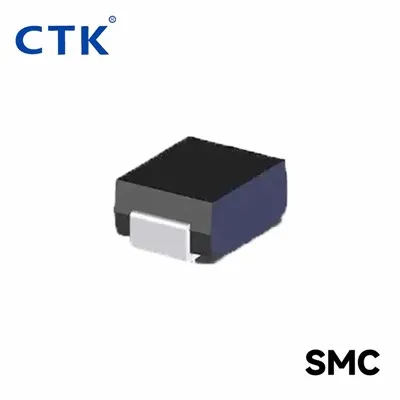
When you choose our ESD protection solutions, you can expect the following benefits:
- High – quality Products: Our products are rigorously tested to ensure they meet the highest standards of ESD protection performance. They can effectively protect your electronic products from ESD damage, reducing the risk of malfunctions and failures.
- Customized Solutions: We understand that different products have different ESD protection requirements. Therefore, we offer customized solutions to meet your specific needs. Our technical team can work with you to design the most suitable ESD protection solutions for your products.
- Excellent Technical Support: Our experienced technical team is always ready to provide you with technical support and advice. Whether you have questions about ESD testing, product selection, or installation, we can offer you professional solutions.
Transistor If you are interested in our ESD protection solutions and would like to discuss your procurement needs, please feel free to contact us. We look forward to working with you to ensure the reliability and performance of your electronic products.
References
- IEC 61000 – 4 – 2: Electromagnetic compatibility (EMC) – Part 4 – 2: Testing and measurement techniques – Electrostatic discharge immunity test.
- ANSI/ESDA/JEDEC JS – 001: Human – body model (HBM) electrostatic discharge test method.
- MIL – STD – 883 Method 3015: Electrostatic discharge sensitivity classification.
Tongke Electronic Co., Ltd
Tongke Electronic Co., Ltd. is one of the most experienced esd manufacturers and suppliers in China, featured by quality products and low price. Please rest assured to wholesale advanced esd made in China here from our factory. Contact us for pricelist.
Address: No.3,Chayuan Rd, Street 3, AilingKan, Dalingshan, Dongguan, Guangdong, China.
E-mail: jack@ctk-elec.com
WebSite: https://www.ctkchip.com/
